


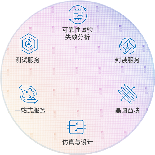


Packaging Solutions

JCET offers a full spectrum of semiconductor packaging services to meet diverse customer needs, spanning lead-frame packaging, substrate-based packaging, flip-chip interconnects, and advanced wafer-level packaging. Our unique advantage lies in its comprehensive wafer-level technology platform, covering Fan-In Wafer-Level Packaging (FIWLP), Fan-Out Wafer-Level Packaging (FOWLP), Integrated Passive Devices (IPD), and Through-Silicon Via (TSV) based interposer solutions. These technologies address the growing demand for next-generation high-density devices, enabling greater integration, enhanced functionality, and smaller form factors.
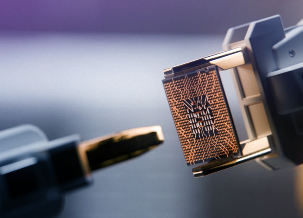
Working side by side with customers on both chip and package design, we deliver products that meet exacting targets for performance, quality, turnaround time, and cost. Our broad wafer-level technology platform gives customers the flexibility to integrate 2.5D and 3D solutions into advanced mobile devices such as smartphones and tablets.

More solutions