
 English
Semiconductor companies are continually faced with complex integration challenges as consumers want their electronics to be smaller, faster and higher performance with more and more functionality packed into a single device. Semiconductor packaging has a significant impact on addressing these challenges. Current and future demands for greater system performance, increased functionality, reduced power consumption and reduced form factor require an advanced packaging approach known as system integration.
System integration is combining multiple integrated circuits (ICs) and components into a single system or modularized sub-system in order to achieve higher performance, functionality and processing speeds with a significant reduction in space requirements inside the electronics device.
What is System-in-Package?
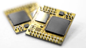
System-in-Package (SiP) is a functional electronic system or sub-system that includes two or more heterogeneous semiconductor die (often from different technology nodes optimized for their individual functionalities), usually with passive components. The physical form of SiP is a module, and depending on the end application, the module could include a logic chip, memory, integrated passive devices (IPD), RF filters, sensors, heat sinks, antennas, connectors and/or power chip in packaged or bare die form.
Advantages of Advanced SiP
To meet the need for increased integration, improved electrical performance, reduced power consumption, faster speed and smaller device sizes, several advantages are driving the industry towards advanced SiP solutions including:
• Thinner / smaller form factor than individually packaged components
• Increased performance and functional integration
• Design flexibilities
• Better electromagnetic interference (EMI) isolation
• Reduced system board space and complexity
• Improved power management and more room for battery
• Simplified SMT assembly process
• Cost effective “plug-and-play” solutions
• Faster time-to-market (TTM)
• One stop turnkey solution – Wafer to fully tested SiP modules
Applications
Today, advanced SiP and miniaturized modules are being utilized in a number of markets such as mobile devices, Internet of Things (IoT), wearables, healthcare, industrial, automotive, computing and communication networks. Each advanced SiP solution varies in complexity based on the number and functionality of the components required by each application.
Following are examples of advanced SiP applications:
• RF power amplifier (PA) modules
• Front-end modules (FEM)
• Power management integrated circuit (PMIC)
• Baseband / application processor (APU)
• High-end application processors (CPU, GPU)
• Connectivity modules
• Fingerprint sensors
• Micro-electromechanical systems (MEMS)
• Solid-state drives (SSD)
Depending on the application requirements and product complexity, there are advanced SiP configurations ranging from conventional 2D modules with multiple active and passive components, interconnected through flip chip, wire bonding and SMT to more complex modules such as Package-in-Package (PiP), Package-on-Package (PoP), 2.5D and 3D integrated solutions. The advanced SiP module configurations (2D/2.5D/3D) are customized for specific end applications to leverage a variety of potential benefits including performance, cost, form factor, and Time-to-Market (TTM).